Physical Vapor Deposition Market Overview
Thin-Film Coating Technology and Advanced Manufacturing Drive PVD Innovation Across Semiconductors, Solar Energy, and Medical Device Industries
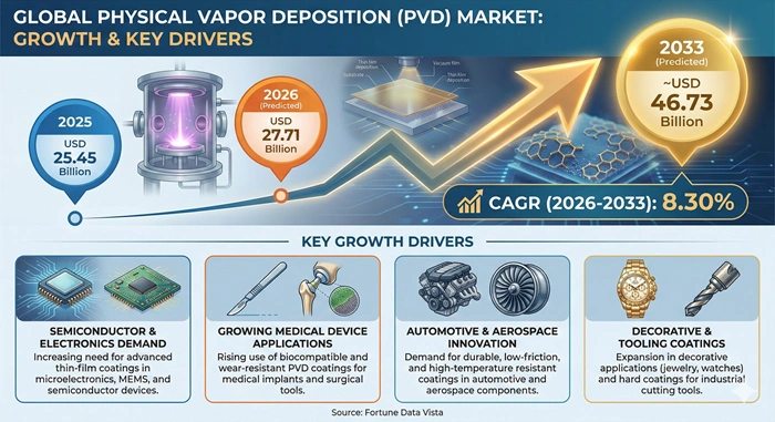
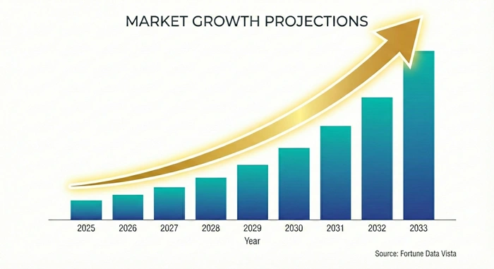
The global physical vapor deposition market size is valued at USD 25.45 billion in 2025 and is predicted to increase from USD 27.71 billion in 2026 to approximately USD 46.73 billion by 2033, growing at a CAGR of 8.30% from 2026 to 2033. This specialized surface engineering sector encompasses production, formulation, and supply of thin-film coating technologies utilizing vacuum-based deposition processes transforming solid materials into vapor phase before condensing onto substrates. The physical vapor deposition market addresses critical performance requirements where functional coatings, wear resistance, and optical properties drive adoption across semiconductors, data storage, cutting tools, medical devices, and solar energy applications requiring reliable coating technology and technical support capabilities.
The physical vapor deposition market benefits from escalating demand for advanced surface engineering solutions where microelectronics, energy storage, and precision manufacturing require thin-film coatings delivering superior hardness, corrosion resistance, and functional properties. PVD processes including sputtering, thermal evaporation, and cathodic arc deposition enable precise control of coating composition, thickness, and microstructure. Major sectors including semiconductor manufacturing, data storage, solar panels, cutting tools, and medical equipment consume substantial PVD coating services as companies pursue operational efficiency, product performance, and sustainability compliance throughout manufacturing operations requiring proven coating technology and application expertise.
AI Impact on the Physical Vapor Deposition Industry
Process Optimization and Quality Control Revolutionize Coating Uniformity and Deposition Efficiency
Artificial intelligence transforms the physical vapor deposition market through advanced process control systems monitoring deposition parameters, coating uniformity, and substrate temperature optimizing coating quality and deposition efficiency across manufacturing operations. Machine learning algorithms analyze thousands of processing variables including chamber pressure, target power, substrate bias, and deposition rate identifying optimal settings achieving target coating thickness, composition uniformity, and adhesion strength while minimizing material usage and energy consumption. These AI-powered platforms enable real-time adjustments preventing coating defects, delamination, and composition variations, reducing raw material losses and improving overall equipment effectiveness particularly critical given stringent performance requirements for semiconductor and medical device applications. Predictive quality models correlating deposition parameters and coating characteristics with final product performance enable proactive interventions maintaining consistent specifications meeting customer expectations and regulatory requirements throughout production cycles.
Advanced AI applications extend beyond manufacturing optimization to revolutionize coating formulation development and performance testing within the physical vapor deposition market landscape. Neural networks analyze coating performance data including hardness, adhesion, and wear resistance predicting optimal formulations, target material selections, and processing conditions achieving desired performance targets. Computer vision systems inspect coated substrates identifying defects, thickness variations, and surface irregularities supporting quality assurance programs and troubleshooting initiatives. Automated testing protocols incorporating hardness measurements, adhesion testing, and corrosion resistance evaluation reduce development cycles from months to weeks enabling rapid process optimization. These AI-driven capabilities position manufacturers to achieve superior operational efficiency while reducing processing costs by 20-30% and improving customer satisfaction throughout forecast period.
Growth Factors
Semiconductor Industry Expansion and Solar Energy Growth Drive Unprecedented Physical Vapor Deposition Adoption
The physical vapor deposition market experiences robust growth propelled by semiconductor industry expansion where integrated circuits, memory devices, and advanced packaging require thin-film coatings enabling miniaturization and performance enhancement. Global semiconductor market projected to exceed 600 billion dollars by 2030 with growing PVD coating consumption demonstrates strong demand fundamentals. Semiconductor applications including logic chips, memory chips, and power devices consume substantial sputtering deposition services requiring specialized coatings offering enhanced conductivity, dielectric properties, and barrier performance. Data storage applications including hard disk drives, solid-state drives, and magnetic recording media require precise thin-film structures. Microelectronics applications including sensors, actuators, and micro-electro-mechanical systems require reliable coating processes enabling miniaturization. These semiconductor applications create sustained baseline demand supporting market growth throughout forecast period.
Solar energy industry growth accelerates physical vapor deposition market expansion as photovoltaic manufacturers require thin-film coatings enabling efficient light absorption and charge separation. Global solar energy market projected to exceed 400 billion dollars by 2030 with growing PVD coating consumption demonstrates strong demand fundamentals. Crystalline silicon solar applications including monocrystalline and polycrystalline panels consume substantial thermal evaporation services. Thin-film solar applications including cadmium telluride, copper indium gallium selenide, and amorphous silicon require specialized deposition processes. Tandem solar applications including perovskite-silicon and multi-junction cells demonstrate growing adoption. These solar energy applications demonstrate exceptional growth supporting sustained consumption throughout forecast period.
Market Outlook
Sustainability Integration and Circular Economy Principles Position Industry for Technology-Driven Transformation
The physical vapor deposition market outlook remains exceptionally positive as manufacturers invest substantially in sustainable coating technologies, circular economy integration, and advanced deposition processes addressing environmental concerns and performance requirements. Next-generation PVD systems incorporating energy-efficient processes, material recycling, and reduced chemical usage deliver improved environmental performance while maintaining or enhancing coating characteristics. Advanced coating systems enable production of recyclable coated products supporting circular economy initiatives and sustainable manufacturing practices. Material recycling technologies utilizing PVD processes enable target material recovery and reuse supporting closed-loop material flows. Sustainable target materials derived from recycled sources create opportunities for environmentally responsible coating production. These sustainability innovations create competitive advantages as semiconductor manufacturers, solar energy producers, and medical device companies increasingly prioritize suppliers demonstrating environmental stewardship throughout forecast period.
Investment trends within the physical vapor deposition market reflect growing confidence in long-term demand fundamentals as equipment manufacturers, coating service providers, and research institutions expand capacity, develop proprietary coating systems, and pursue strategic partnerships. Leading manufacturers including Applied Materials, Lam Research, ASM International, and regional producers maintain capital expenditure programs modernizing deposition facilities, implementing advanced chamber designs, and developing application-specific coating portfolios. Acquisition activity intensifies as specialty equipment companies pursue market consolidation through strategic acquisitions of coating technology platforms, intellectual property portfolios, and customer relationships. Vertical integration strategies connecting equipment manufacturing with coating services and technical support create comprehensive solution offerings. Research collaborations advancing novel target materials, improved deposition uniformity, and enhanced coating performance support market evolution balancing performance requirements with sustainability imperatives through 2033.
Expert Speaks
-
Applied Materials Leadership, emphasized technology advancement: "Our advanced physical vapor deposition systems deliver superior coating uniformity, exceptional process efficiency, and reduced environmental footprint. These innovative PVD platforms enable semiconductor manufacturers, solar energy producers, and cutting tool companies to achieve enhanced product performance, operational cost reductions, and sustainability targets without compromising coating quality standards".
-
Lam Research Management, highlighted sustainability imperative: "The transition to sustainable thin-film coating represents a strategic imperative for manufacturing transformation. Our PVD equipment provides exceptional deposition control, improved environmental profile, and regulatory compliance supporting customer sustainability commitments, circular economy integration, and environmental protection objectives throughout electronics manufacturing value chains".
-
ASM International Leadership, articulated innovation direction: "Next-generation physical vapor deposition technology revolutionizes thin-film engineering enabling precise coating architecture control, enhanced material efficiency, and diversified application opportunities. This platform supports semiconductor innovation, solar energy enhancement, and advanced medical device applications demonstrating commitment to innovation excellence and customer value creation".
Key Report Takeaways
-
Asia Pacific dominates the physical vapor deposition market with commanding share exceeding 51%, driven by extensive semiconductor manufacturing, solar panel production, and electronics assembly across China, Japan, South Korea, and Taiwan where government support programs, advanced manufacturing initiatives, and export-oriented production create substantial PVD coating consumption supporting regional economic development.
-
North America emerges as fastest-growing regional market with projected CAGR approaching 8.8% through 2033, propelled by semiconductor industry expansion, advanced manufacturing growth, medical device development, and aerospace applications where government investment programs, technology leadership, and innovation ecosystem create concentrated coating demand supporting regional economic competitiveness.
-
Sputtering deposition represents dominant process segment accounting for approximately 58% market share due to proven performance, versatility, and widespread adoption across semiconductor manufacturing demonstrating sustained consumption across logic chips, memory devices, and data storage applications requiring reliable coating solutions.
-
Cathodic arc deposition exhibits fastest technology growth with projected CAGR exceeding 9.6% through 2033, attributed to superior coating properties, enhanced adhesion, and premium application suitability where cutting tools, medical implants, and specialty products drive adoption supporting segment expansion.
-
Microelectronics applications maintain largest application segment representing approximately 46% of market driven by operational efficiency, performance advantages, and miniaturization supporting large-scale semiconductor manufacturing across integrated fabrication facilities and dedicated coating service providers.
-
Solar energy applications demonstrate exceptional growth potential with anticipated CAGR of 9.2% through 2033, driven by renewable energy mandates, photovoltaic technology advancement, and cost reduction where crystalline silicon, thin-film solar, and tandem cells create concentrated coating demand supporting continued segment leadership.
Market Scope
| Parameter | Details |
|---|---|
| Market Size by 2033 | USD 46.73 Billion | Market Size by 2026 | USD 27.71 Billion | Market Size by 2025 | USD 25.45 Billion | Market Growth Rate from 2026 to 2033 | CAGR of 8.30% | Dominating Region | Asia Pacific | Fastest Growing Region | North America | Segments Covered | Process Type, Application, End-Use Industry, Region | Regions Covered | North America, Europe, Asia Pacific, Latin America, Middle East & Africa |
Market Dynamics
Drivers Impact Analysis
Semiconductor Industry Growth and Renewable Energy Expansion Accelerate Physical Vapor Deposition Adoption
| Impact Factor | (≈) % Impact on CAGR Forecast | Geographic Relevance | Impact Timeline |
|---|---|---|---|
| Semiconductor Industry Expansion | +3.2% | Global Markets | 2026-2033 |
| Solar Energy Growth | +2.8% | Developed Regions | 2026-2033 |
| Medical Device Industry Growth | +2.4% | Asia Pacific | 2026-2033 |
| Cutting Tool Demand | +2.0% | Global Markets | 2026-2033 |
The physical vapor deposition market benefits substantially from semiconductor industry expansion where integrated circuits, memory devices, and advanced packaging require thin-film coatings enabling miniaturization and performance enhancement. Global semiconductor market projected to exceed 600 billion dollars annually by 2030 with growing PVD coating consumption demonstrates strong demand fundamentals. Semiconductor applications including logic chips, memory chips, and power devices consume substantial sputtering deposition services requiring specialized coatings offering enhanced conductivity, dielectric properties, and barrier performance. Data storage applications including hard disk drives, solid-state drives, and magnetic recording media require precise thin-film structures. Microelectronics applications including sensors, actuators, and micro-electro-mechanical systems require reliable coating processes enabling miniaturization. These semiconductor applications create sustained baseline demand supporting market growth throughout forecast period.
Solar energy industry growth accelerates physical vapor deposition market adoption as photovoltaic manufacturers require thin-film coatings enabling efficient light absorption and charge separation. Global solar energy market projected to exceed 400 billion dollars annually by 2030 with growing PVD coating consumption demonstrates strong demand fundamentals. Crystalline silicon solar applications including monocrystalline and polycrystalline panels consume substantial thermal evaporation services. Thin-film solar applications including cadmium telluride, copper indium gallium selenide, and amorphous silicon require specialized deposition processes. Tandem solar applications including perovskite-silicon and multi-junction cells demonstrate growing adoption. These solar energy applications demonstrate exceptional growth supporting sustained consumption throughout forecast period.
Restraints Impact Analysis
Equipment Complexity and High Initial Investment Constrain Market Penetration Across Price-Sensitive Segments
| Restraint Factor | (≈) % Impact on CAGR Forecast | Geographic Relevance | Impact Timeline |
|---|---|---|---|
| High Capital Investment | -1.4% | Global Manufacturing | 2026-2033 |
| Technical Complexity | -1.2% | Developed Markets | 2026-2031 |
| Maintenance Requirements | -0.8% | Price-Sensitive Applications | 2026-2030 |
| Alternative Technology Competition | -0.6% | Sustainability-Focused Markets | 2027-2033 |
The physical vapor deposition market faces growth constraints from high capital investment requirements where specialized vacuum equipment, deposition chambers, and target materials create financial barriers and implementation challenges. Domain-specific knowledge requirements for process optimization, coating design, and equipment maintenance create talent gaps particularly in emerging markets with limited surface engineering education infrastructure. Maintenance requirements including target replacement, chamber cleaning, and vacuum system servicing create operational burdens. Training requirements for operators, technicians, and engineers create additional investment burdens. These capital dynamics create implementation challenges particularly for small and medium enterprises throughout forecast period.
Technical complexity constrains physical vapor deposition market development where process expertise, application knowledge, and quality control requirements create implementation barriers. Domain-specific knowledge requirements for coating design, deposition parameter optimization, and substrate preparation create talent gaps particularly in emerging markets with limited materials science education infrastructure. Application requirements including coating adhesion, thickness uniformity, and composition control create technical challenges. Training requirements for operators, technicians, and engineers create additional investment burdens. These technical dynamics create implementation challenges particularly for specialized coating applications throughout forecast period.
Opportunities Impact Analysis
Circular Economy Integration and Advanced Technologies Create Substantial Growth Avenues Beyond Traditional Applications
| Opportunity Factor | (≈) % Impact on CAGR Forecast | Geographic Relevance | Impact Timeline |
|---|---|---|---|
| Circular Economy Technologies | +2.0% | Developed Markets | 2027-2033 |
| Advanced Energy Storage | +1.8% | Sustainability-Focused Regions | 2028-2033 |
| Flexible Electronics | +1.4% | Advanced Manufacturing | 2026-2033 |
| Emerging Market Growth | +1.2% | Asia Pacific, Africa | 2026-2033 |
The physical vapor deposition market stands to capture substantial value from circular economy technologies where target material recycling enables recovery and reuse of precious metals and rare earth elements supporting closed-loop material flows. Advanced recycling technologies recovering coating materials from end-of-life products create opportunities for PVD processes optimized for recycled content integration. Material recovery processes benefiting from PVD-enabled thin-film structures supporting multiple recycling cycles without significant property degradation demonstrate growing adoption. Circular economy facilities utilizing specialized PVD coatings for product longevity, material efficiency, and recyclability create concentrated demand. Brand owner commitments to circular economy targets driving investment in sustainable manufacturing infrastructure support coating innovation. Government incentives promoting circular economy development, waste reduction, and resource efficiency create favorable regulatory environment. These recycling applications command premium positioning and demonstrate exceptional growth supporting market diversification throughout forecast period.
Advanced energy storage production presents exceptional growth opportunities as battery manufacturers, supercapacitor producers, and fuel cell developers require thin-film coatings enabling efficient charge storage and transfer. Advanced battery technologies derived from lithium-ion, solid-state, and next-generation chemistries enable energy storage utilizing PVD coatings. Physical vapor deposition processes optimized for energy storage addressing coating uniformity, interface engineering, and material compatibility create technical differentiation. Electric vehicle manufacturers pursuing energy density targets, fast charging capabilities, and lifecycle performance prioritize advanced thin-film coatings. Grid storage operators implementing renewable energy integration consider PVD-coated electrodes for performance enhancement. Government mandates promoting electrification, reduced fossil fuel dependence, and clean energy transition support market development. These sustainable alternatives command premium pricing and demonstrate growing adoption supporting market expansion throughout forecast period.
Segment Analysis
By Process Type: Sputtering Deposition
Versatility and Established Technology Sustain Sputtering Market Leadership Across Semiconductor Applications
Sputtering deposition commands the largest share within the physical vapor deposition market, accounting for approximately 58% of global consumption with continued expansion projected at steady CAGR of 7.8% through 2033. This process category encompasses magnetron sputtering, ion beam sputtering, and reactive sputtering techniques bombarding target materials with energetic ions ejecting atoms that deposit onto substrates. The physical vapor deposition market benefits from sputtering advantages including proven performance, excellent coating uniformity, broad material compatibility, and precise composition control supporting widespread adoption across semiconductor manufacturing. Fourth-generation sputtering systems incorporating advanced magnetron designs, plasma control, and high-power impulse techniques deliver superior coating quality and deposition rates. Reactive sputtering processes enabling compound coating formation maintain market leadership despite growing adoption of cathodic arc alternatives. Large-scale and batch processing utilizing sputtering deposition dominate commercial semiconductor fabrication.
Asia Pacific and North America lead sputtering deposition consumption within the market, driven by extensive semiconductor manufacturing, data storage production, and display fabrication. Taiwan Semiconductor Manufacturing Company, Samsung, and Intel consume substantial sputtering services across advanced logic and memory production. United States semiconductor facilities including Arizona and Texas fabrication plants demonstrate consistent coating demand. Chinese semiconductor expansion including new fabrication facilities utilizes sputtering deposition for capacity growth and technology advancement. Leading equipment manufacturers including Applied Materials, Lam Research, and ASM International maintain sputtering technology platforms serving semiconductor producers. Technology improvements including high-power impulse magnetron sputtering, improved target utilization, and reduced particle generation extend process capabilities. Process versatility supporting sputtering preferences over specialized thermal evaporation alternatives maintains segment dominance throughout forecast period.
By Application: Microelectronics
Performance Requirements and Miniaturization Position Microelectronics Segment for Sustained Market Leadership
Microelectronics applications represent dominant segment within the physical vapor deposition market, accounting for approximately 46% of total consumption with continued expansion projected at robust CAGR of 8.4% through 2033. This application category encompasses integrated circuits, memory devices, sensors, and micro-electro-mechanical systems requiring advanced thin-film coatings enabling device functionality and performance. The physical vapor deposition market benefits from microelectronics advantages including superior coating quality, precise thickness control, and material purity supporting large-scale semiconductor manufacturing. Logic chip applications including processors, graphics processing units, and application-specific integrated circuits consume substantial sputtering deposition services. Memory applications including dynamic random-access memory, flash memory, and emerging memory technologies require specialized coating processes. Sensor applications including image sensors, pressure sensors, and biosensors demonstrate growing adoption. Other microelectronics including power devices and radio frequency components create concentrated demand.
Asia Pacific and North America lead microelectronics-related physical vapor deposition consumption within the market, driven by extensive semiconductor fabrication, technology leadership, and miniaturization requirements. Taiwan semiconductor capacity including TSMC and United Microelectronics Corporation predominantly utilizes sputtering deposition demonstrating established infrastructure. Korean semiconductor expansion including Samsung and SK Hynix facilities implements advanced PVD processes supporting capacity growth and node advancement. United States manufacturers maintaining semiconductor technologies demonstrate continued investment in equipment upgrades. Leading equipment licensors including Applied Materials licensing proprietary chambers, Lam Research offering advanced deposition systems, and Tokyo Electron providing integrated solutions maintain market positions. Process advantages including atomic-level thickness control, multi-layer capability, and pattern fidelity support continued technology adoption. Performance benefits including improved device performance and reliability align with semiconductor roadmap objectives supporting segment leadership throughout forecast period.
Regional Insights
Asia Pacific
Manufacturing Concentration and Technology Leadership Establish Regional Dominance in Physical Vapor Deposition Market
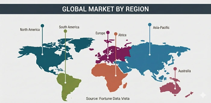
Asia Pacific commands the physical vapor deposition market with dominant share exceeding 51%, driven by extensive semiconductor manufacturing, solar panel production, and electronics assembly across China, Japan, South Korea, and Taiwan where government support programs, advanced manufacturing initiatives, and export-oriented production create substantial PVD coating consumption. Taiwan alone accounts for approximately 35% of Asia Pacific market share with semiconductor foundry capacity exceeding 60% global market share supporting logic chips, memory devices, and specialty applications. South Korean semiconductor sector demonstrating rapid growth particularly memory production and display manufacturing creates growing coating demand. Chinese solar panel manufacturers maintaining global leadership demonstrate consistent consumption. Japanese semiconductor equipment producers operating advanced facilities maintain substantial demand supporting regional market position.
Regional industrial policies strengthen Asia Pacific's market position through manufacturing incentives, technology development, and export promotion supporting semiconductor industry development. Taiwanese government programs emphasizing semiconductor leadership, manufacturing excellence, and supply chain resilience maintain substantial physical vapor deposition equipment investment and coating service growth. South Korean government initiatives including semiconductor mega clusters and technology development zones promote domestic equipment manufacturing capabilities. Chinese government programs supporting semiconductor self-sufficiency, innovation leadership, and manufacturing scale advance coating technology development. Leading regional equipment manufacturers including Tokyo Electron, SCREEN Holdings, and Ulvac maintain supply chains serving semiconductor producers. The region's market dominance continues through 2033 as manufacturing growth, technology advancement, and capacity expansion create sustained demand supporting continued leadership throughout forecast period.
North America
Technology Innovation and Advanced Manufacturing Drive Fastest Regional Market Growth
North America emerges as fastest-growing regional physical vapor deposition market with projected CAGR of 8.8% through 2033, propelled by semiconductor industry expansion, advanced manufacturing growth, medical device development, aerospace applications, and technology innovation where government investment programs, CHIPS Act funding, and innovation ecosystem create concentrated coating demand. United States semiconductor reshoring including Intel, Texas Instruments, and GlobalFoundries capacity expansion demonstrates growing consumption. Canadian medical device sector including implants and surgical instruments creates concentrated demand. Mexican aerospace manufacturers including aircraft components and engine parts operating integrated facilities maintain substantial demand. Government investment programs including CHIPS and Science Act funding, infrastructure initiatives, and manufacturing incentives create favorable conditions. Leading equipment companies investing in regional production facilities, research centers, and customer support capabilities position for market leadership. The region's exceptional growth continues through 2033 as reshoring, technology leadership, and strategic priorities create favorable dynamics supporting sustained market expansion throughout forecast period.
Top Key Players
-
Applied Materials Inc. (United States)
-
Lam Research Corporation (United States)
-
ASM International N.V. (Netherlands)
-
Tokyo Electron Limited (Japan)
-
ULVAC Inc. (Japan)
-
Veeco Instruments Inc. (United States)
-
Kurt J. Lesker Company (United States)
-
Advanced Energy Industries Inc. (United States)
-
Oerlikon Balzers (Liechtenstein)
-
IHI Corporation (Japan)
-
AJA International Inc. (United States)
-
Angstrom Engineering Inc. (Canada)
-
Denton Vacuum LLC (United States)
-
Impact Coatings AB (Sweden)
-
Singulus Technologies AG (Germany)
Recent Developments
-
Applied Materials Inc. (2024-2025): Launched advanced Endura sputtering system achieving superior coating uniformity through enhanced magnetron design and plasma control optimization, demonstrating leadership enabling semiconductor manufacturers and solar panel producers to achieve enhanced product performance, operational cost reductions, and sustainability targets while expanding equipment sales to Asian semiconductor fabs supporting technology adoption across emerging process nodes.
-
Lam Research Corporation (2024-2025): Expanded physical vapor deposition equipment portfolio including next-generation VECTOR systems providing exceptional deposition control, improved throughput, and regulatory compliance, implementing advanced chamber designs and plasma technologies while securing long-term supply agreements with major semiconductor manufacturers supporting technology roadmap advancement and manufacturing scale throughout forecast period.
-
ASM International N.V. (2024-2025): Advanced PVD platform enabling precise thin-film architecture control, enhanced material efficiency, and diversified application opportunities demonstrating technology leadership in semiconductor innovation, advanced packaging, and emerging memory technologies while establishing strategic partnerships with foundries and integrated device manufacturers supporting market penetration and customer value creation.
-
Tokyo Electron Limited (2023-2024): Completed strategic investments in sputtering technologies strengthening market position in advanced semiconductor manufacturing, developing sustainable coating processes including energy-efficient systems and material recycling capabilities while expanding technical services providing process optimization, equipment installation, and customer training supporting semiconductor producers pursuing productivity improvements and technology transitions.
-
Applied Materials Inc. (2023-2025): Expanded equipment production capacity in United States and Singapore adding 30% additional manufacturing capability addressing growing semiconductor fabrication demand and reshoring opportunities, implementing Industry 4.0 technologies and automated assembly systems while developing proprietary chamber designs competing with regional equipment suppliers supporting American semiconductor self-sufficiency and competitiveness objectives.
Market Trends
Sustainability Integration and Advanced Technologies Reshape Industry Competitive Dynamics
The physical vapor deposition market experiences transformative trends centered on sustainability integration as circular economy principles, energy efficiency mandates, and environmental consciousness drive innovation toward green coating processes and material recycling. Manufacturers develop PVD systems enabling energy consumption reduction, target material recycling, and reduced chemical usage supporting sustainable manufacturing infrastructure. Material recovery technologies utilizing specialized recycling processes for precious metals, rare earth elements, and strategic materials create closed-loop material flows. Renewable energy-powered PVD facilities utilizing solar and wind energy demonstrate growing commercialization. Reduced environmental footprint coating processes minimizing waste generation, eliminating hazardous materials, and improving material efficiency support sustainability objectives. Life cycle assessment methodologies quantifying environmental impacts, carbon footprints, and resource efficiency inform equipment development and customer selection. These sustainability initiatives create competitive advantages as semiconductor manufacturers, solar energy producers, and medical device companies increasingly prioritize suppliers demonstrating environmental stewardship throughout forecast period.
Atomic layer deposition integration trends reshape the physical vapor deposition market as hybrid deposition approaches combining PVD and ALD techniques deliver superior coating conformality, composition control, and nanoscale precision. Hybrid formulations enabling precise thickness control, conformal coverage, and interface engineering produce high-performance coatings competing with single-process approaches. Advanced packaging applications utilizing hybrid deposition delivering exceptional gap-fill capability, barrier performance, and thermal management support three-dimensional integration. Sequential processing technologies combining sputtering and atomic layer deposition in integrated clusters optimize throughput and cost-effectiveness. Post-deposition treatment development including plasma enhancement and thermal annealing expands coating capabilities. Intellectual property landscape surrounding hybrid technologies influences market dynamics and competitive positioning. These advanced coating approaches command premium pricing, demonstrate growing adoption, and support market differentiation enabling equipment manufacturers to capture value in high-performance semiconductor segments throughout forecast period.
Segments Covered in the Report
By Process Type
-
Sputtering Deposition (Magnetron Sputtering, Ion Beam Sputtering, Reactive Sputtering)
-
Thermal Evaporation (Electron Beam Evaporation, Resistive Evaporation)
-
Cathodic Arc Deposition (Arc Evaporation, Filtered Arc Deposition)
-
Other Processes (Ion Plating, Pulsed Laser Deposition)
By Application
-
Microelectronics (Integrated Circuits, Memory Devices, Sensors)
-
Data Storage (Hard Disk Drives, Solid State Drives, Magnetic Recording)
-
Solar Products (Crystalline Silicon, Thin-Film Solar, Tandem Cells)
-
Cutting Tools (Drills, End Mills, Inserts)
-
Medical Equipment (Implants, Surgical Instruments, Diagnostic Devices)
By End-Use Industry
-
Semiconductor Industry (Logic Chips, Memory Devices, Power Devices)
-
Solar Energy Industry (Photovoltaics, Concentrated Solar, Hybrid Systems)
-
Cutting Tool Industry (Metalworking, Woodworking, Construction)
-
Medical Device Industry (Orthopedic, Cardiovascular, Dental)
-
Others (Automotive, Aerospace, Decorative Coatings)
By Region
-
North America (United States, Canada, Mexico)
-
Europe (Germany, France, United Kingdom, Italy, Spain, Rest of Europe)
-
Asia Pacific (China, Japan, South Korea, Taiwan, India, Rest of Asia Pacific)
-
Latin America (Brazil, Argentina, Rest of Latin America)
-
Middle East & Africa (Saudi Arabia, UAE, South Africa, Rest of MEA)
Frequently Asked Questions:
Answer: The global physical vapor deposition market is expected to reach approximately USD 46.73 billion by 2033, growing from USD 27.71 billion in 2026. This substantial expansion reflects semiconductor industry growth, solar energy expansion, medical device sector development, and coating technology advancement across diverse thin-film applications worldwide.
Answer: Asia Pacific leads the physical vapor deposition market with over 51% share, driven by extensive semiconductor manufacturing, solar panel production, and electronics assembly across China, Japan, South Korea, and Taiwan. Leading equipment manufacturers including Applied Materials, Tokyo Electron, and ULVAC maintain dominant positions serving regional semiconductor producers and coating service providers.
Answer: Key growth drivers include semiconductor industry expansion requiring thin-film coatings for miniaturization, solar energy growth supporting photovoltaic manufacturing, medical device industry development enabling biocompatible coatings, and cutting tool demand promoting wear-resistant surfaces. Circular economy initiatives promoting material recycling and sustainable manufacturing create additional market opportunities throughout forecast period.
Answer: Sputtering deposition dominates the physical vapor deposition market with approximately 58% share due to versatility, proven performance, and widespread adoption across semiconductor manufacturing. These processes support logic chips, memory devices, and data storage applications demonstrating sustained consumption across advanced technology nodes requiring precise coating control.
Answer: Environmental regulations drive sustainable equipment development addressing energy consumption, material efficiency, and waste management requirements. Semiconductor manufacturers, solar energy producers, and medical device companies increasingly prioritize suppliers demonstrating environmental compliance and sustainability credentials. These regulatory pressures create opportunities for innovative coating technologies while promoting energy-efficient processes supporting market transformation throughout forecast period.
